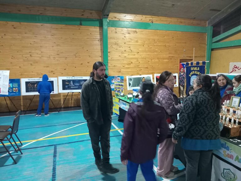



As part of Children and Adolescents’ Heritage Day, organized by the Municipality of Santiago, the Center for Nanoscience and Nanotechnology (CEDENNA) will present its traveling exhibition “Images of the Nanoworld”, a unique exhibition that reveals the invisible wonders of matter at the nanoscale. Taking part will be National Prize for Exact Sciences winner Dora Altbir, and the director of the CEDENNA Center Program, Juliano Casagrande, who will talk with the public.
This Saturday, August 23, the Municipality of Santiago will celebrate Children and Adolescents’ Heritage Day with a cultural and educational day at the Plaza de Armas, featuring various activities open to the community.
In this context, the municipality invited CEDENNA to set up its exhibition in front of the city hall building, where it will remain during the day and will then be displayed inside.
The exhibition belongs to the CEDENNA Foundation and will feature the participation of its director, Dr. Dora Altbir, 2019 National Prize for Exact Sciences winner, and Dr. Juliano Casagrande, director of the CEDENNA Center Program, who will be present to talk with the public, answer questions and share the contributions of nanotechnology.
A window to the invisible world
For more than a decade, CEDENNA has organized an internal contest in which its researchers capture surprising images of the nano world using high-end electron microscopy. These photographs show structures invisible to the human eye, many of which evoke fantastic landscapes, marine forms or abstract figures.
The exhibition, made up of 12 selected images, offers scientific descriptions in language accessible to all audiences. Among them, for example:
- Butterfly: a porous hydrogel that, under the microscope, reveals shapes that look like the wings of a butterfly in full spring flight.
- Microcrystal crosses: tiny vanadium oxide crystals that, as they grew, formed a perfect cross, as if nature had played with invisible geometric figures.
- Nanocoral: microscopic tubes that naturally organize into structures very similar to a marine coral.
- Pink jellyfish: titanium dioxide crystals that evoke the silhouette of jellyfish floating in an imaginary ocean.
- Hanging nanobridges: nanometric filaments connecting different areas, looking like bridges suspended in the air.
- Magnetic nanosphere: a tiny sphere made of cobalt atoms that shines like a microscopic jewel.
Traveling science for all of Chile
“Images of the Nanoworld” has toured various cities in the country, including Antofagasta, Arica, Iquique, Valparaíso and Santiago, as well as universities and cultural centers such as the USACH Planetarium, the Bellas Artes Metro Station, the Universidad de Tarapacá, Universidad Diego Portales and Puerto de Ideas’ Paseo por la Ciencia 2025.
Its tour has brought science closer to thousands of people of all ages, showing that nanotechnology not only drives innovation in health, energy or the environment, but can also be an aesthetic and cultural experience.
“Behind this beauty in the nanouniverse there are many practical things, because each of these particles has a concrete use, for example, to remove arsenic from water, to improve the quality of food packaging, to absorb oxygen so that food does not oxidize and lasts longer, in a mining sensor or to detect pathogens in food”, highlights Dr. Altbir.
This exhibition seeks to spark the curiosity and interest of audiences of all ages in nanotechnology, which includes applications developed from the new properties materials exhibit at the nanoscale. Some applications have existed for a long time and range from sunscreens to paints with specific properties, including components in our computers and cell phones, as well as revolutionary cancer treatments.
A nanometer is one millionth of a millimeter, which is why nanometer-sized systems can only be observed with specialized microscopy.